top of page
All productions are complied with the ISO and UL Standards and committed to IPC, as the guideline for the acceptability, as well as ISO/TS16949 by the International Automotive Task Force (IATF)
Production Approvals
Technical Capabilites
IPC definies several type of via structure
IPC Standard Paper
Example of PCB Stack Up Design
Factory Visit
Brief view of the facility

PTH.jpg
Plated pcb, printed circuit board, Printed circuit board, Circuit Imprime, Circuits imprimés

Plating.jpg
Plated pcb, printed circuit board, Printed circuit board, Circuit Imprime, Circuits imprimés

Etching.jpg
Etching pcb, printed circuit board, Printed circuit board, Circuit Imprime, Circuits imprimés
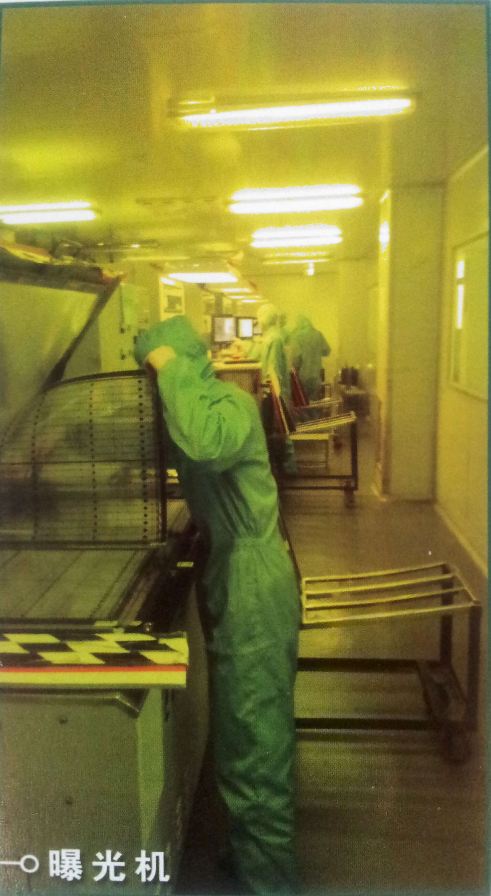
Exposure.jpg
Exposure pcb, printed circuit board, Printed circuit board, Circuit Imprime, Circuits imprimés
1/1
 Combining Rogers and FR4 in layer stackup |  Pre‐Preg Thickness Style# 1080 = 3.04 mil Style# 2116 = 4.67 mil Style# 7628 = 7.68 mil For the above design, it can be 1*7628+1 *1080 or 2*2116. |  It takes 4 sheets of pre-preg for the above design. |
|---|---|---|
 A typical PCB stackup is constructed from multiple alternating layers of core, prepreg, and copper foil materials heat-pressed and glued together. |  The design above represent standard multi-layer PCB stack up carried by 2 sheets of pre-preg. |
bottom of page